
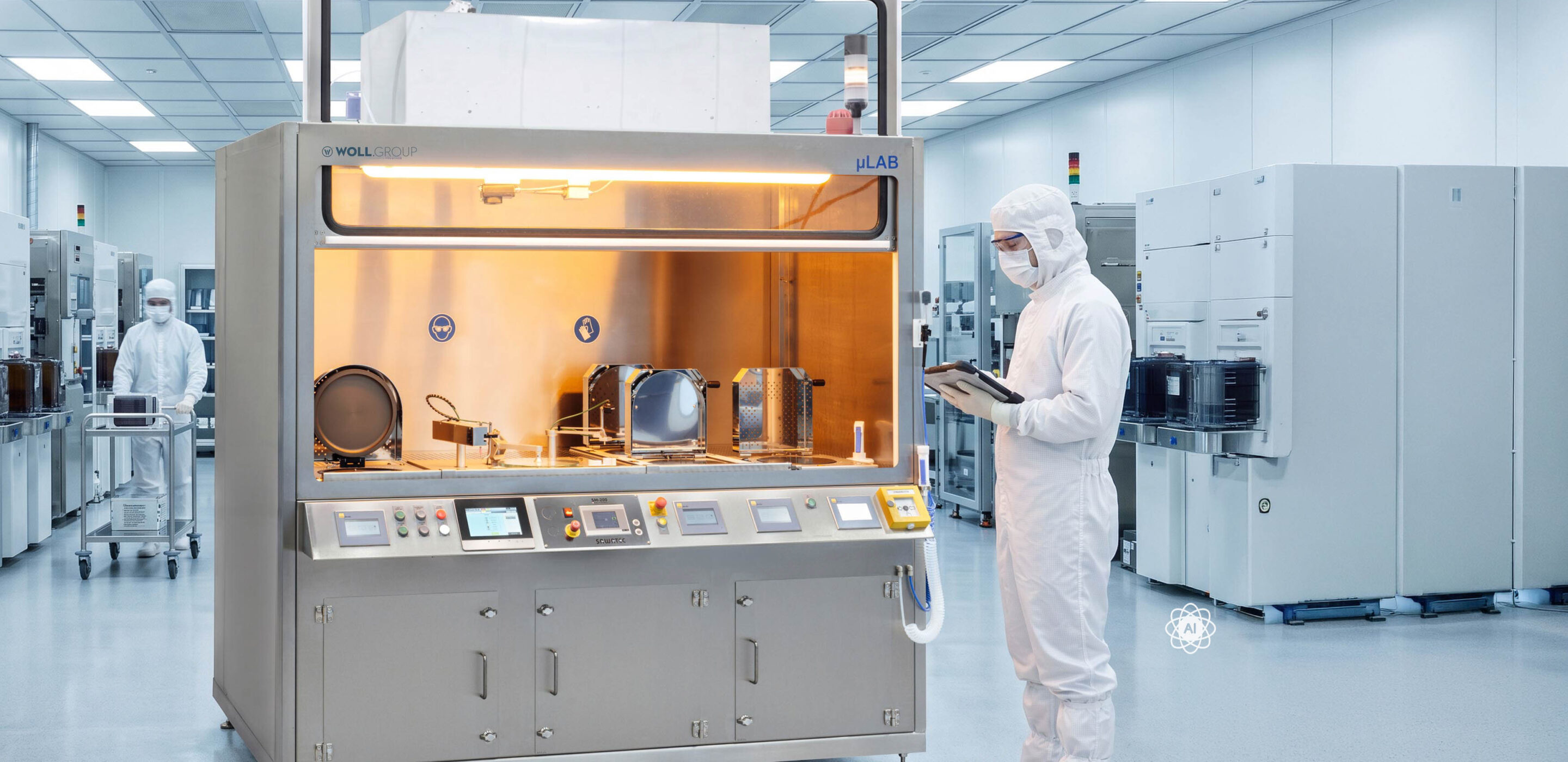
Photoresist processing
with μLAB and μCHEM
Photoresist processing is a process-critical component of semiconductor manufacturing and is key to the precise definition of micro- and nanostructured wafers. As demands on resolution, process window, and reproducibility increase, stable and tightly controlled wet-chemical process steps are increasingly coming into focus.
The μCHEM and μLAB systems are designed for precise and reproducible photoresist processing across the entire wet-chemical process chain. They support coating, developing, etching, and cleaning of photoresist layers under tightly controlled conditions and are designed for flexible adaptation to varying process requirements in development and production.
Typical applications include wet-chemical photoresist processes in semiconductor manufacturing, wafer patterning for MEMS and sensor systems, and development and qualification processes for new photoresists. In addition, the systems enable implementation of customer-specific process flows with well-defined and stable process windows.
Your advantages
- High process stability and reproducibility across all wet-chemical photoresist steps
- Precise control of process parameters for tight tolerances and stable results
- High flexibility with resist types, substrates and process sequences
- Suitable for R&D, pilot processes and industrial production
- Modular and automatable system concepts for integration into existing process environments
System solutions
for photoresist processing
Photoresist processing > µLAB
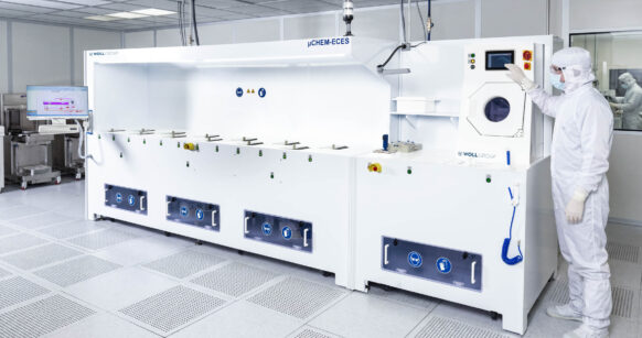
Wet etching system > µCHEM

Select the right system solution!
We support you in configuring μCHEM and μLAB for your application.
WOLL.GROUP
T +49 681 992 727 9 – 0
info@m-o-t.info