
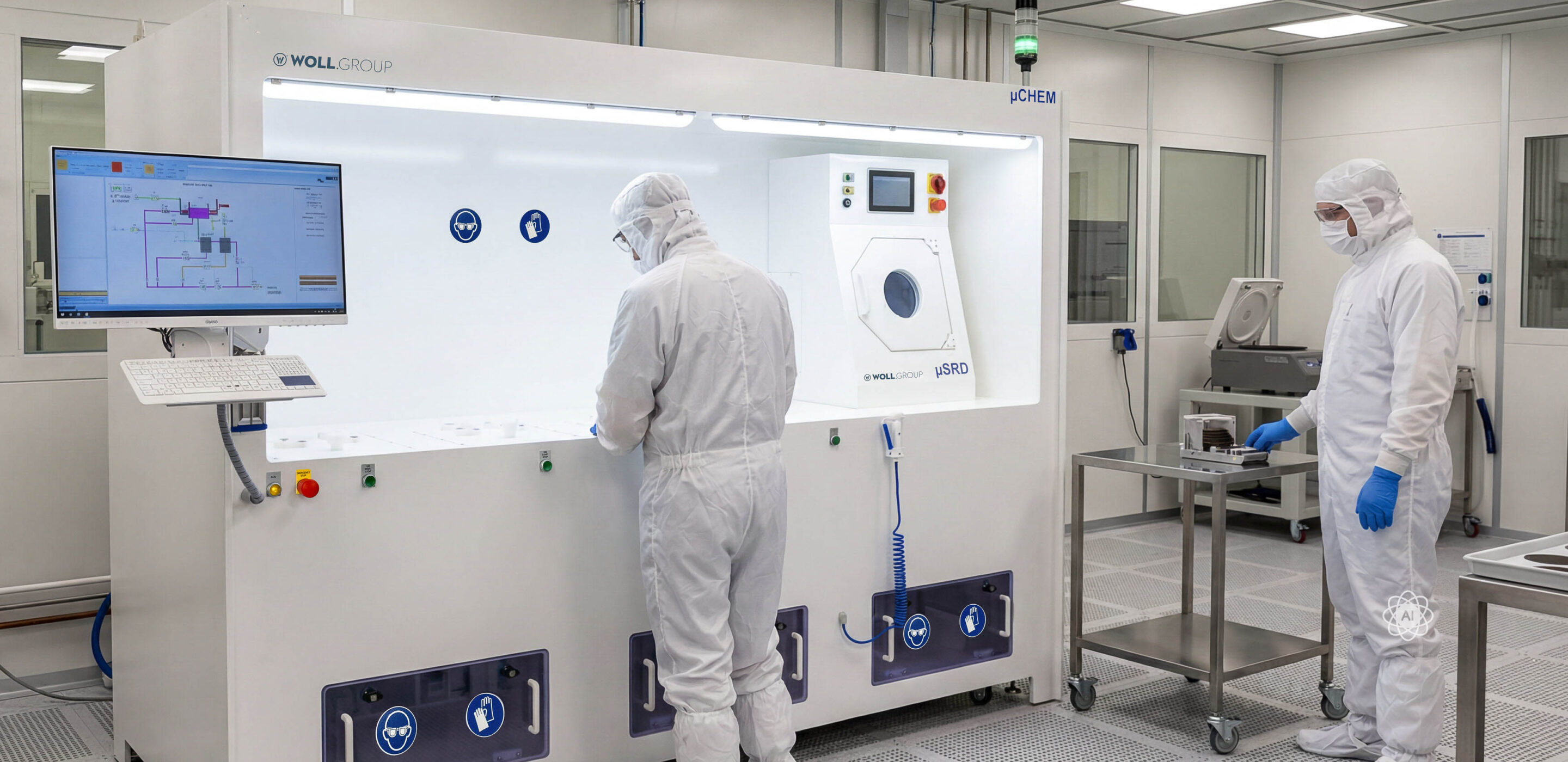
Innovative etching technology
for precise wafer processes
Etching processes are a central element of semiconductor manufacturing and are crucial for the precise definition of complex structures on wafer surfaces. The high demands on structural fidelity, reproducibility, and process stability require high-performance etching systems with tightly controlled process parameters.
We develop customized etching solutions for demanding applications in development and production. The systems are designed for the use of high-purity etching chemicals and precise, stable process control, ensuring high consistency – both in high-volume manufacturing and in specialized, application-specific processes.
The portfolio includes automated etching systems and modular system concepts that can be seamlessly integrated into existing manufacturing environments. Typical applications range from customer-specific etching processes with tight process windows and the structuring of semiconductor wafers to etching processes for MEMS and sensor systems, as well as precision etching for micro- and nanostructured components.
Your advantages
- Precise process control for consistent etching results
- Use of high-purity etching chemicals for maximum process reliability
- Automatable system concepts for development and production environments
- Scalable from specialized applications to large-scale production
System solutions
for etching technology
Below are selected example systems that illustrate our technological solutions in etching processes. They demonstrate how we realize precise, stable, and integrable systems for demanding wafer processes.
Wet etching system μCHEM
Electrochemical etch stop μCHEM-ECES

Porosification µPORSI

Find the right etching process!
WOLL.GROUP
T +49 681 992 727 9 – 0
info@m-o-t.info